OUR WORK
Covering ATE engineering to mass production, CP probe cards, loadboards / burn-in boards, EVB / PCB design, package design, and supporting hardware (stiffeners, tooling, sockets) — a full-spectrum case showcase.
Covering mainstream ATE platforms, supporting engineering verification, debug and mass-production operation
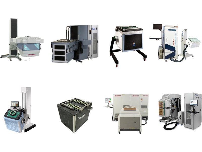
Production test services backed by a fleet of V93K/T5833/T5503HS2, UltraFlex Plus/UltraFlex/J750, STS8300/STS8200, Chroma 3380P, and S100 machines — ensuring capacity and on-time delivery.
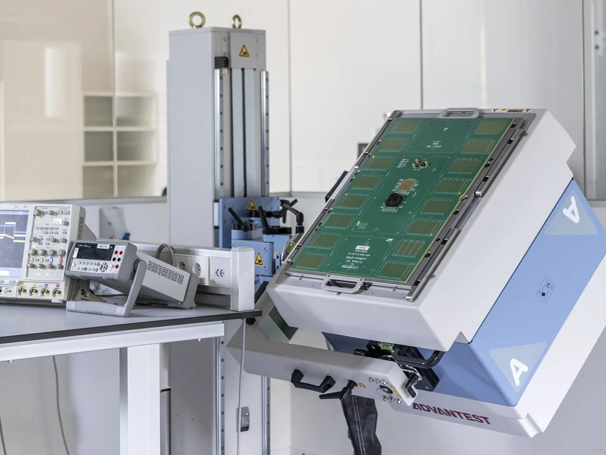
Supporting engineering verification, debug, and production ramp-up across mainstream test platforms — V93K, T5833/T5503HS2, T2000/C2000, UltraFlex/J750, STS8300/STS8200, Chroma 3380P, and ytec S100.
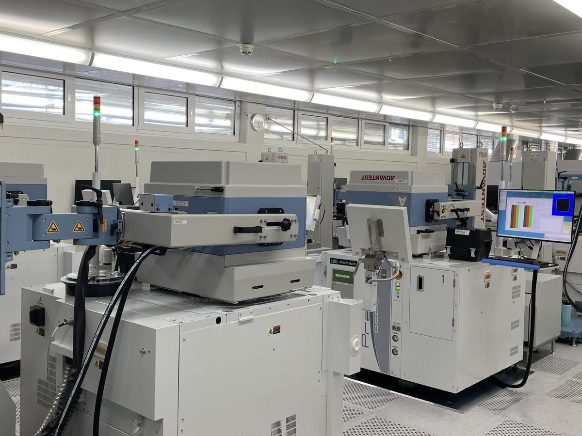
A full ATE fleet covering the complete CP and FT flow, with tri-temperature (ambient / hot / cold) testing for high-volume production.
Cantilever and vertical probe cards for wafer sort (CP), supporting multi-site parallel testing
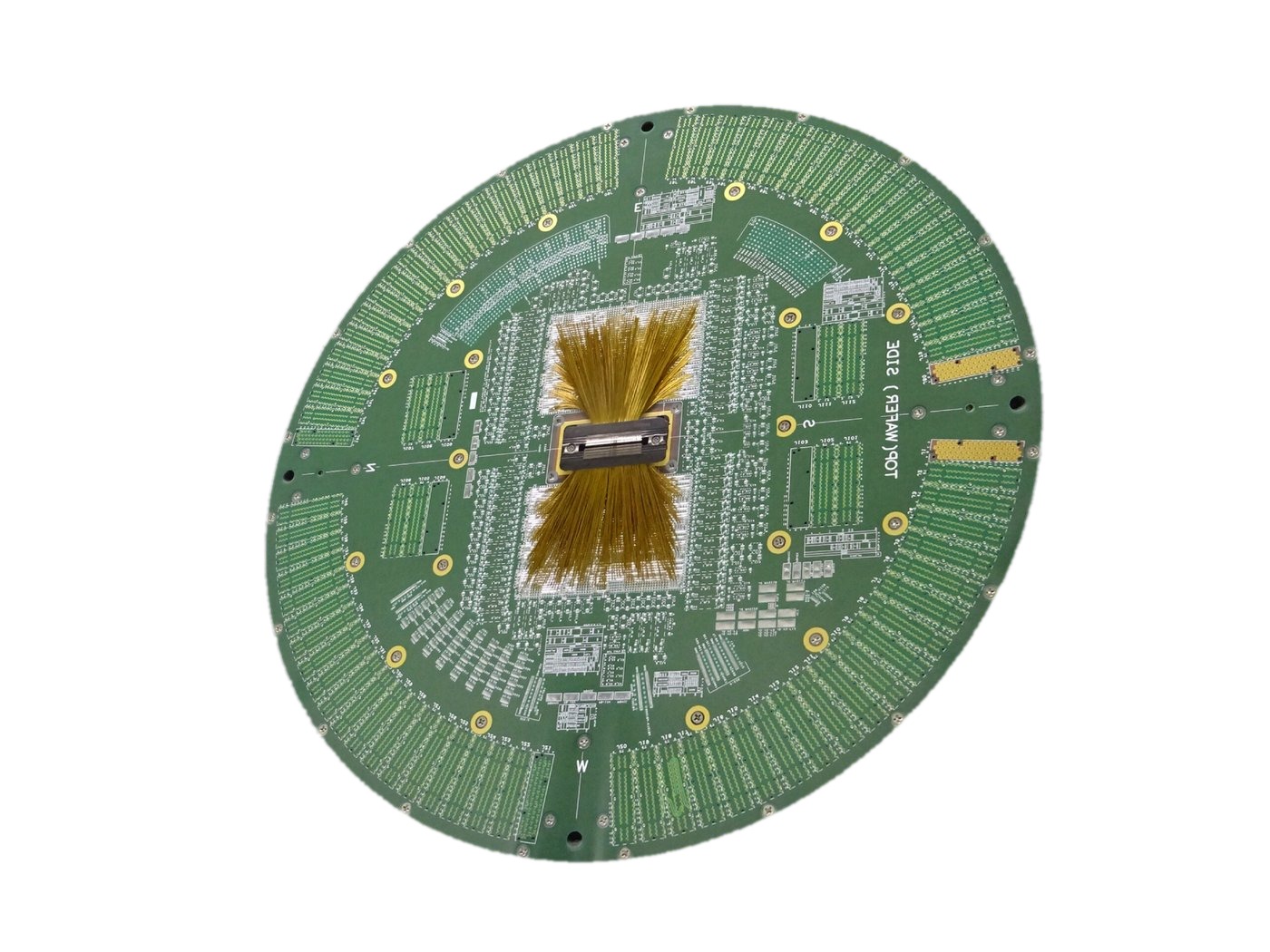
Cantilever probe cards for wafer sort (CP), supporting multi-site parallel testing with stable contact resistance and long probe life.
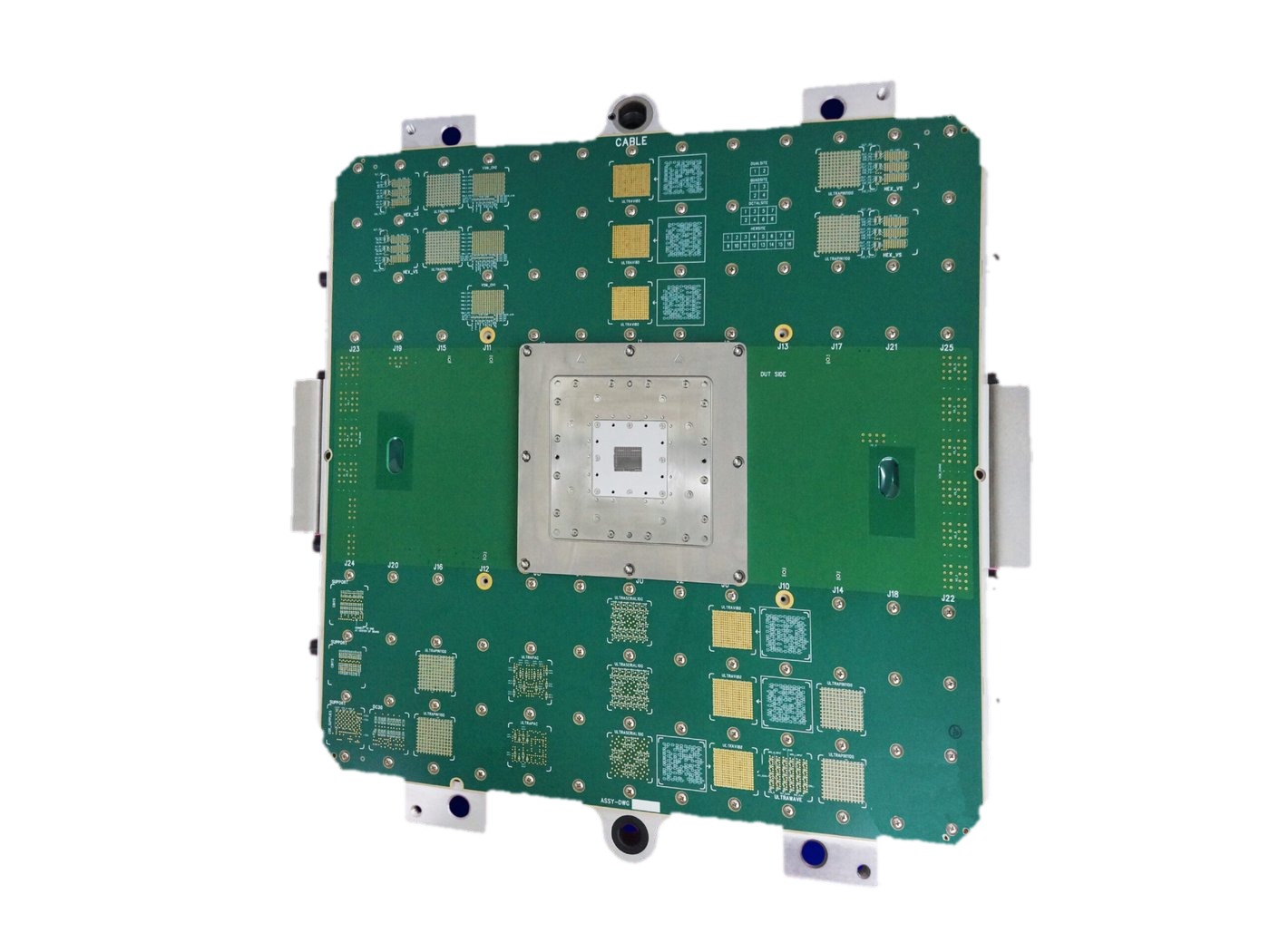
VPC vertical probe card design and manufacturing, suited for high-pin-count, fine-pitch wafer testing with multi-site parallel efficiency.
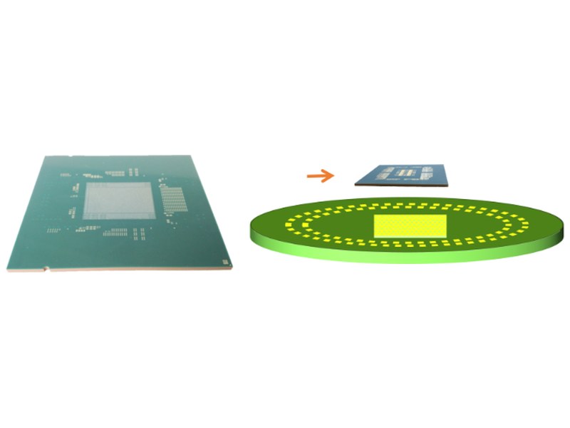
Design and manufacturing of 20–32 layer MLO test substrates — high-density multilayer routing and multi-site arrays for parallel testing, balancing signal integrity and reliability.
Loadboards for mainstream ATE platforms — Advantest / Teradyne / Accotest / Chroma — plus multi-site Burn-in Board design and manufacturing
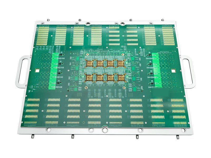
Production loadboard for the Advantest V93K platform, with high-speed signal integrity design and optimized high-current power channels.
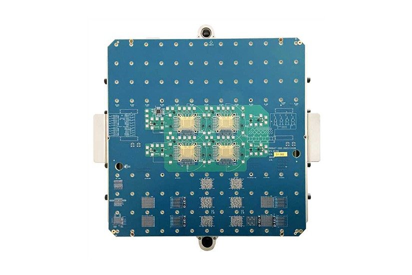
Production loadboard for the Chroma 3380P platform, targeting power management and analog device testing.
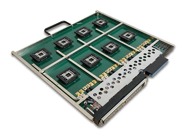
High-density routing and multi-site socket arrays for ambient and high-temperature long-duration burn-in, delivered turnkey from design, SMT, to assembly test.
EVB, demo and system boards for AI / GPU / storage / SoC and 112G / 224G SerDes
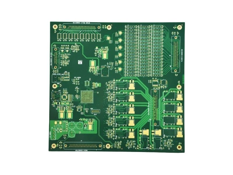
High-speed PCB design, simulation and signal integrity optimization for 112G / 224Gbps SerDes, PCIe and CPO products.
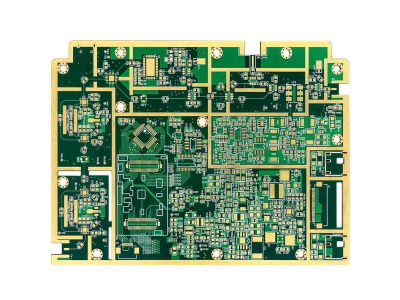
System control board — from schematic and layout to fabrication and assembly, engineered for high reliability and production stability.
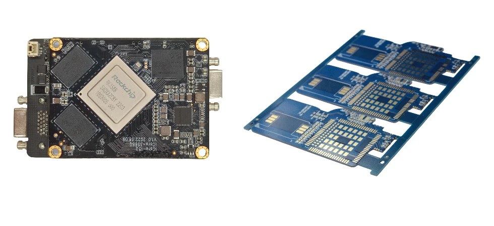
Machine vision board — from schematic and layout to fabrication and assembly, engineered for high-speed image processing and production reliability.
Handler change kits and IC test sockets for fast conversion across package types in volume production
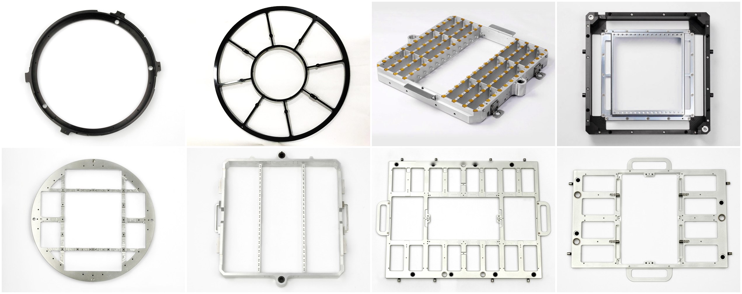
Design and manufacturing of stiffeners and docking boards in round, square and multi-site layouts, providing rigid support and precise positioning for test loadboards.
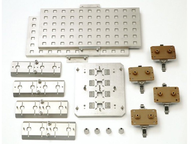
Change kits for pick & place / gravity test handlers, covering socket guides, trays and contact chucks for fast conversion across package types in volume production.
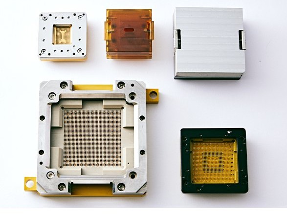
IC test sockets for BGA / QFN / LGA packages, with spring-probe and Kelvin contact options balancing high-speed signal integrity and long contactor life.
A one-stop supply-chain service spanning package and substrate co-design, foundry tape-out, and packaging from prototyping through volume production
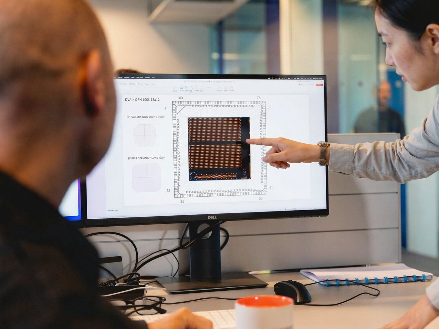
With professional packaging partners, we cover everything from QFN, DFN, BGA to WLCSP and SiP — tailoring the most cost-effective, application-fit package for every ASIC, balancing mechanical, thermal, and electrical needs.
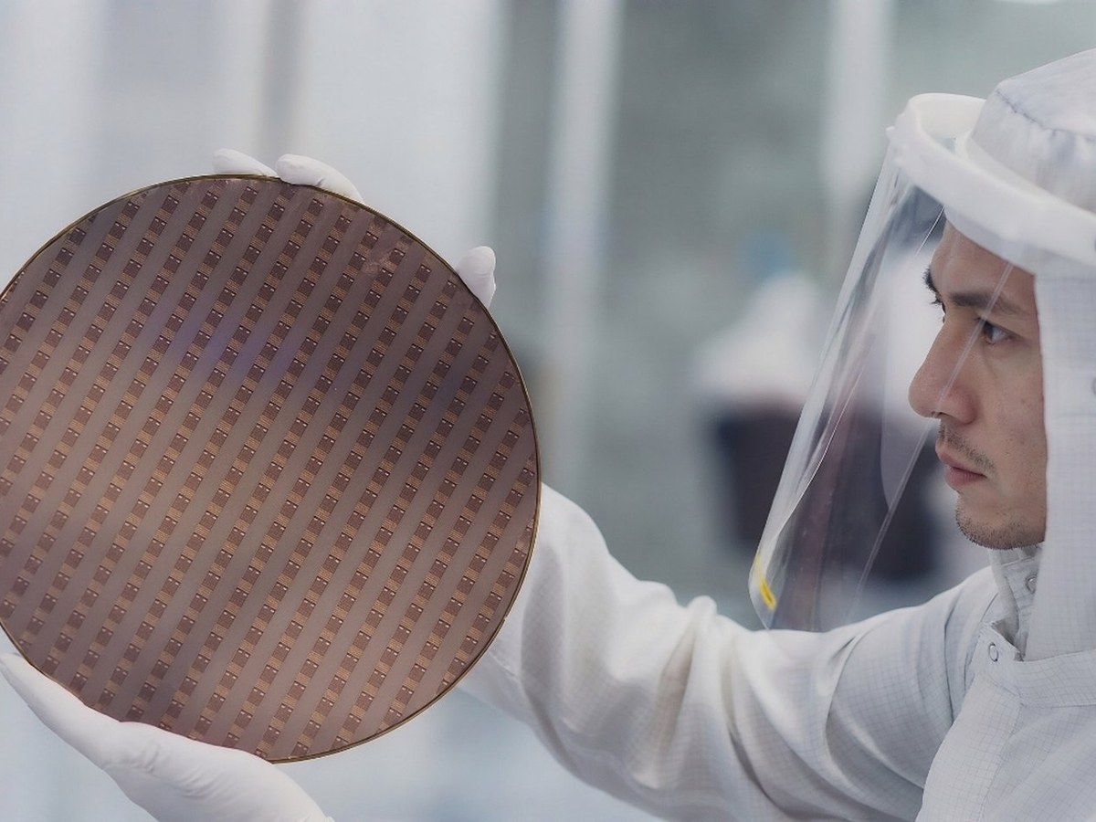
Backed by an established foundry network, we provide fully managed tape-out support across mature to advanced nodes (180nm to 5nm), precisely matching the right process for any custom or high-end chip — with 20+ successful tape-outs, delivered secure, compliant, and on time.
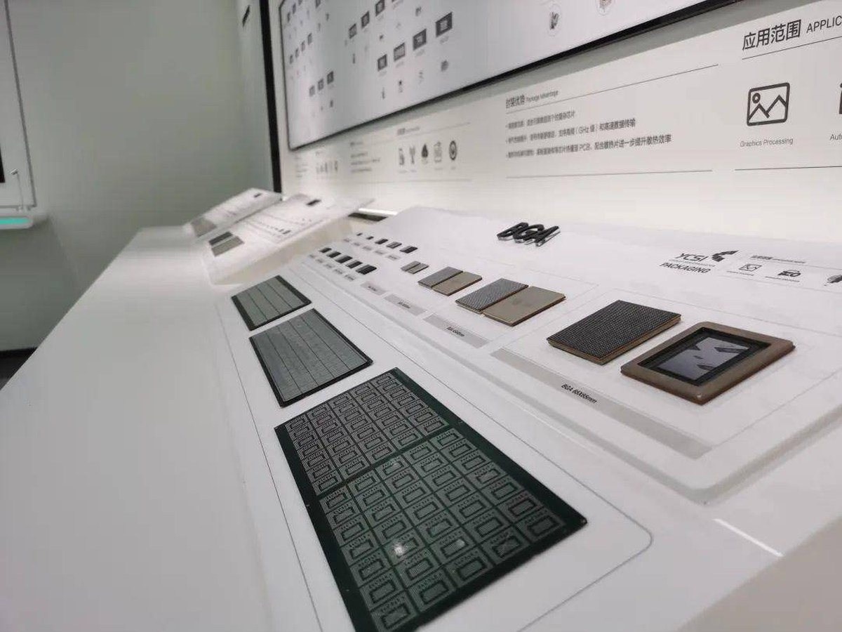
Built on a differentiated OSAT network, we deliver fully managed support from package selection and DFM to prototyping and volume production, helping customers choose the right solution, raise yield, and control cost — fast at small scale, assured at volume.
For more case information, contact business@ptest.cn.